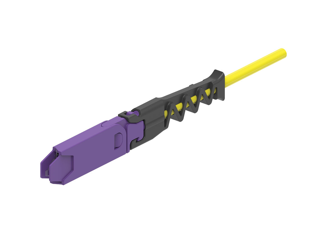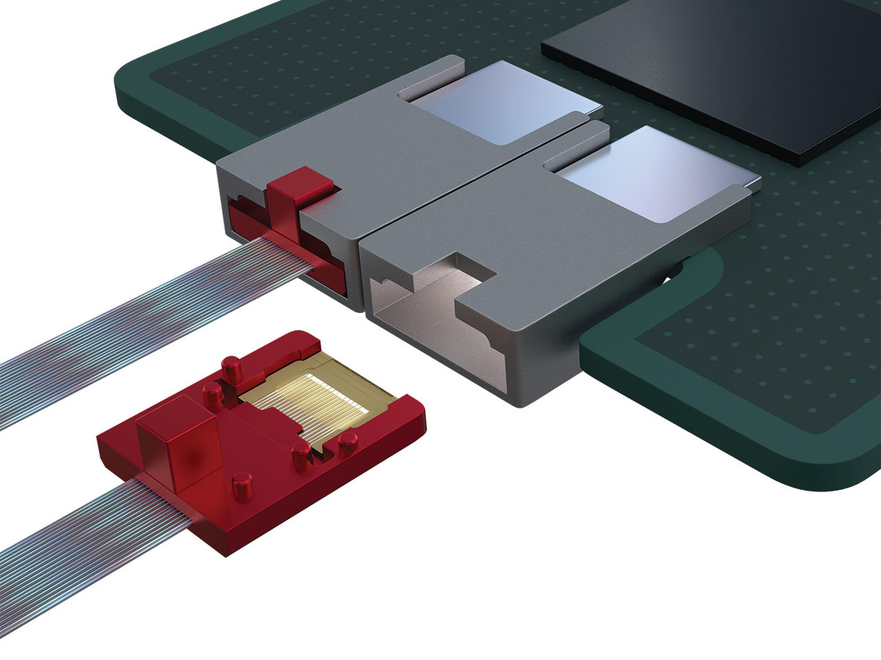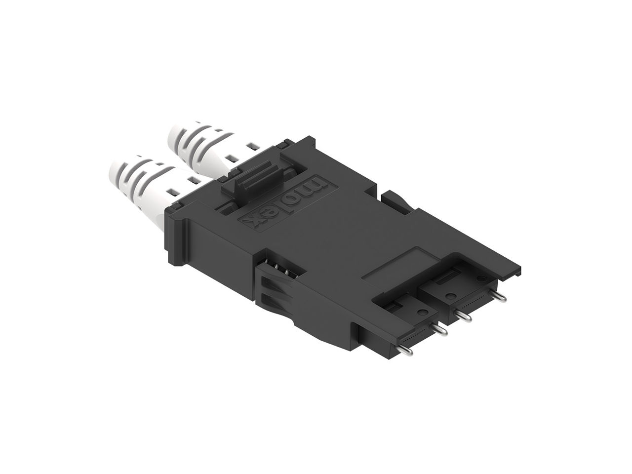

| Fiber Types | Optical Coupling | Density | Serviceability |
|---|---|---|---|
| SM and PM | Surface Coupling to PICs using either inverse tapered waveguides (wideband) or grating couplers (narrowband) | Up to 50 fibers at 127μm pitch per Photonic-Plug. Several Photonic-Plugs can be connected to a single PIC using a modular socket design. | Post-reflow fiber connectivity through a serviceable, detachable Photonic-Plug |
Features and Benefits
As AI, hyperscale and high-performance computing systems continue to scale, connecting increasing numbers of high-density optical fibers to silicon photonics chips presents a growing challenge. Precise alignment requirements increase manufacturing complexity and cost, while traditional fiber attachment methods limit scalability as channel counts increase and make high-volume deployment more difficult. Once integrated into a package, fiber-to-chip interfaces are often difficult to service, replace and test, making it difficult to maintain manufacturing yield and operational reliability.
To overcome the challenges of scaling optical connectivity, customers need passive optical alignment technologies that provide broad assembly tolerances. They also need proven semiconductor-compatible manufacturing processes that support high-volume production and repeatability. In addition, serviceable and testable optical connectivity architectures are essential to simplify repair and validation throughout the product lifecycle.
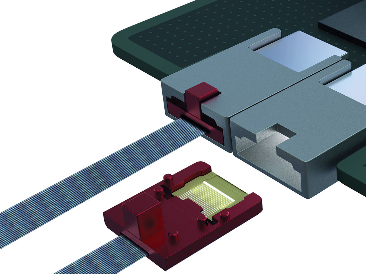
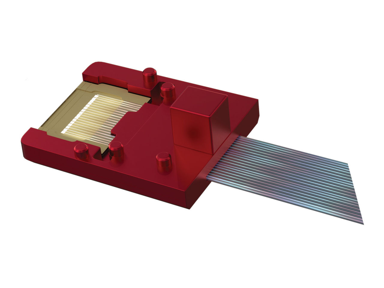
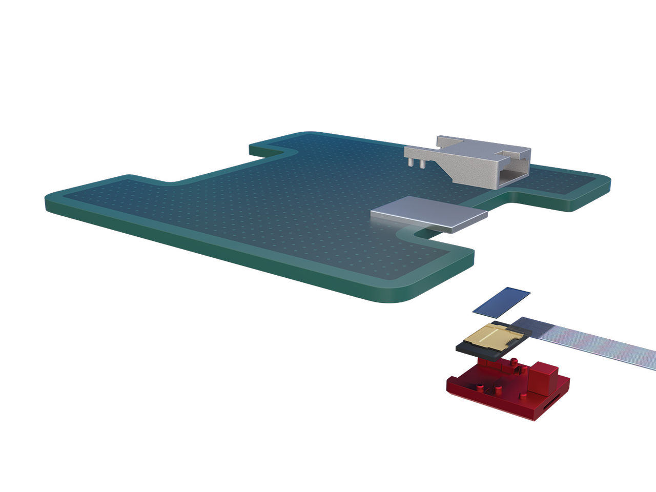
The TeraVERSE system addresses these challenges with self-aligning optics architecture that enables passive alignment and wide assembly tolerances to reduce assembly complexity, lower manufacturing costs, improve yield and enable scalable production. The Photonic-Bump attached to the PIC, deflects the light from the PIC waveguides to its surface, enabling wafer-level testability, to significantly improve manufacturing testability and yield. The detachable, serviceable Photonic-Plug, which enables post-reflow fiber attachment, greatly simplifies CPO manufacturing, increasing manufacturing yield and throughput, and helps push down manufacturing costs. In addition, compatibility with high-volume manufacturing semiconductor packaging flows help improve manufacturing repeatability and support high-volume commercialization.
Applications by Industry
This is not a definitive list of applications for this product. It represents some of the more common uses.
Frequently Asked Questions
What are TeraVERSE Detachable Connectors?
The TeraVERSE Detachable Optical Chiplet Connector is a high-density, detachable and serviceable fiber connector platform for creating a surface-coupled optical interface between fiber and a PIC. It is composed of a detachable Photonic-Plug, Photonic-Bump and mechanical socket that help support scalable fiber-to-chip connectivity for CPO packages.
Does the TeraVERSE system require active alignment?
No, the TeraVERSE connector is designed around patented self-aligning optics for a pure passive alignment with wide assembly tolerances.
What fiber types do TeraVERSE connectors support?
The TeraVERSE system supports both SM and PM fibers.
Why is detachability important?
Detachability allows fibers to be attached after reflow processes and disconnected for servicing, helping improve manufacturability, yield and repairability.
What applications are TeraVERSE connectors optimized for?
The TeraVERSE connector system is optimized for AI infrastructure, hyperscale data centers and high-performance computing applications. It also supports silicon photonics packaging and CPO systems.
Is the TeraVERSE system intended for CPO or pluggable optics?
The TeraVERSE system is optimized for NPO, CPO and other silicon photonics applications that require optical fibers to connect to the PIC.
What optical handoffs do TeraVERSE connectors support?
TeraVERSE connectors support surface coupling from either inverse tapered waveguides for wideband surface coupling or grating couplers for narrowband surface coupling.
What should I confirm before selecting TeraVERSE connectors?
Before selecting TeraVERSE connectors, confirm your PIC’s SiPh Foundry, the PIC coupling type, package geometry, fiber types, channel count, pitch, operating band, front/back-panel termination, target insertion loss and serviceability requirements.