
In most cases, application of a connector has to do with soldering (except crimp and IDT connections). That is why one of the first questions I ask, when it comes to the connector choice is:
What does your solder process look like?
The answer to this question gives me choices and prevents me from recommending the wrong product. Molex tries to explain a lot on the web – either in the product description or in the product specification – however, when it comes to lead-free solder processes (>+250°C for 5 seconds) it is key to know the process in detail.
Is it wave solder? Is it SMT reflow? Does the customer prefer pin-in-paste?
I survived cases where the customer reduced the lead-free wave solder temperature to prevent melted pegs underneath the board (and created un-sufficient solder joints). Make sure to use only products with nickel underplate of the tin plated leads in a lead free environment.
I also saw melting housings, which let the pins drop down when another customer changed from lead to lead-free soldering temperatures. In this case we had to explain the difference between solder temperature and heat resistance, although clearly indicated in the product specification.
We investigated movements of microminiature components during reflow soldering which reminded me of some Hollywood movies taken in a crematory.
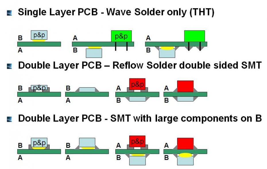
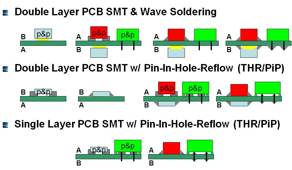
So, knowing the solder process is key for every connector sales person as well as for every user of connectors, here is an overview of various solder processes.
Standard are single layer and double layer pure processes (wave solder or SMT reflow):